
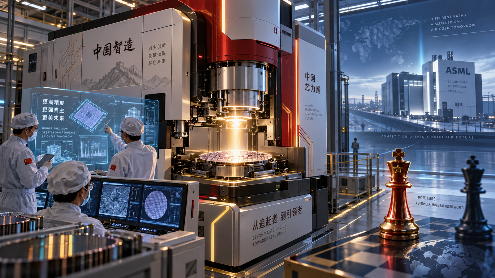
For more than a decade, one company has occupied perhaps the most strategically important position in the global semiconductor industry. The Netherlands-based ASML is the only company in the world currently capable of supplying extreme ultraviolet, or EUV, lithography systems for commercial semiconductor manufacturing. These extraordinarily complicated machines are essential to the economical production of the most advanced chips made by TSMC, Samsung and Intel.
That technological position has made ASML one of the central pressure points in Western attempts to restrict China’s semiconductor development. China has been prevented from acquiring EUV systems, while export controls have progressively restricted access to some of ASML’s most capable deep ultraviolet, or DUV, machines as well. Yet the assumption that denying China EUV would permanently prevent it from manufacturing advanced semiconductors is looking increasingly questionable. China has not yet produced a genuine commercial equivalent of ASML’s EUV platform, but it is pursuing several technological routes simultaneously: stretching DUV lithography far beyond its conventional limits, manufacturing its own immersion-DUV systems, localising the optical and laser components on which lithography depends, and researching alternative approaches to generating EUV light. In effect, China is trying to make ASML’s monopoly progressively less strategically decisive.
ASML’s Monopoly Is Real – But Narrower Than It Sounds
It is important first to define what ASML actually monopolises. ASML itself acknowledges that it is currently the world’s only supplier of EUV lithography technology. EUV uses light with a wavelength of approximately 13.5 nanometres, allowing extremely small structures to be patterned onto silicon with fewer exposures than would be possible using conventional DUV techniques. ASML: Busting ASML myths
But ASML does not have a literal monopoly over semiconductor lithography in general. Japanese companies such as Nikon and Canon remain active in older lithography technologies, and China has long produced less advanced lithography equipment of its own. The strategically important monopolies are ASML’s position in EUV and its overwhelming technological lead in the most advanced immersion-DUV scanners. That distinction matters because EUV is not the only possible way to produce small semiconductor features. It is the most efficient industrial solution currently available, and China has increasingly focused on exploiting the difference.
Huawei and SMIC Demonstrated the DUV Workaround
The most important demonstration came with Huawei’s Mate 60 Pro in 2023. When semiconductor-analysis company TechInsights dismantled the phone, it discovered that Huawei’s Kirin 9000S processor had been fabricated by Semiconductor Manufacturing International Corporation, or SMIC, using a second-generation 7nm-class manufacturing process. The significant part was not simply that China had produced a 7nm chip. It was that SMIC had done so without EUV.
TechInsights subsequently described the Kirin 9000S as the first commercial advanced system-on-chip it had identified from a Chinese foundry using such an advanced process without EUV lithography. TechInsights analysis of the Kirin 9000S process
Instead of EUV, SMIC relied on 193nm immersion-DUV lithography combined with sophisticated multiple-patterning techniques. Rather than printing a highly complex layer in a single exposure, a manufacturer divides the pattern into several simpler operations, repeatedly exposing, depositing and etching the wafer until the desired structures emerge. This is considerably more complicated than using EUV. Every additional patterning step introduces opportunities for alignment errors and defects, increases wafer-processing time, consumes more materials and equipment capacity, and generally makes manufacturing more expensive. But “more expensive” is very different from “impossible”.
Earlier semiconductor generations had already demonstrated this principle. TSMC, Intel and others manufactured early 7nm-class devices using extensive DUV multi-patterning before EUV became widely established. China is effectively taking that technological branch further.
Multipatterning Turns Old Machines Into More Capable Machines
One particularly important technique is self-aligned quadruple patterning, or SAQP. SAQP creates additional features through deposition and etching rather than relying exclusively on the optical resolution of the lithography scanner. In simplified terms, one comparatively coarse lithographic pattern can be transformed into multiple much finer structures. This makes it possible to manufacture dimensions much smaller than the nominal resolution of the lithography machine itself.
Chinese semiconductor-equipment company SiCarrier has been associated with patents involving advanced DUV multipatterning, while Chinese fabs have continued working on processes that could extend non-EUV manufacturing towards 5nm-class devices. The trade-off is economics. Using perhaps three, four or more process stages where an EUV-equipped manufacturer can perform one means more machines, more fabrication time, more opportunities for defects and potentially lower yield. A DUV-produced 5nm chip therefore does not necessarily compete economically with a 5nm chip manufactured at TSMC using EUV.
But the calculation changes when technological sovereignty matters more than wafer cost. For Huawei, Chinese AI companies and potentially the Chinese state, a domestically accessible chip costing substantially more to manufacture may still be preferable to a more advanced foreign chip that cannot legally be purchased at all. This is one reason export controls can have an unusual economic effect: they change the definition of what constitutes an economically viable technology.
China Is Now Building Its Own Immersion-DUV Machines
The next stage is more consequential. Until recently, China’s ability to push DUV beyond its conventional limits still depended significantly on imported lithography systems. That dependency is now beginning to be addressed.
In July 2026, Reuters reported that China had begun production of domestically developed immersion-DUV lithography equipment. The programme is associated with Shanghai Aishengna Electronic Technology Group and engineering teams connected to Yuliangsheng and Shanghai Micro Electronics Equipment, better known as SMEE. Initial machines are intended for Chinese semiconductor manufacturers including SMIC, Hua Hong and memory producer CXMT. Reuters: China starts production of home-grown immersion DUV chipmaking tools
The machines should not be confused with ASML’s newest scanners. They remain technologically behind ASML equipment, and getting a lithography prototype to expose wafers is considerably easier than achieving the overlay accuracy, uptime, throughput and reliability required for continuous high-volume semiconductor production. Nevertheless, this represents an important transition. Lithography is no longer simply a laboratory localisation project for China; domestic immersion-DUV equipment is beginning to enter the manufacturing ecosystem.
More recent reporting by the Financial Times has described Huawei as playing a coordinating role in this effort, backing companies involved not only in complete lithography systems but also in the components required to build them. Yuliangsheng-developed DUV machines are reportedly undergoing testing involving companies including Huawei and SMIC. Financial Times: Huawei drives China’s push to make advanced chips That may ultimately prove more important than any single scanner.
Recreating ASML Means Recreating an Ecosystem
An ASML lithography machine is not simply an ASML product in the conventional sense. Its capabilities depend on a huge international network of specialist suppliers accumulated over decades. ASML says its broader ecosystem encompasses thousands of partners and suppliers. ASML on its technology and supplier ecosystem
Carl Zeiss SMT produces extraordinarily precise optical systems. TRUMPF supplies high-powered laser technology. Cymer, acquired by ASML, became central to the development of EUV light sources. Numerous specialist companies contribute vacuum equipment, precision stages, sensors, mirrors, metrology systems, chemicals and control technologies. China therefore cannot achieve genuine lithography independence merely by assembling a scanner-shaped machine. It has to reproduce much of the industrial ecosystem surrounding the scanner.
That process is now clearly under way. The Financial Times reports that Huawei-linked investment is supporting Chinese companies working on projection optics and high-powered light sources, including Fujian Zhiqi Photonics and Beijing RSLaser Opto-Electronics. These are precisely the kinds of technological bottlenecks that previously made a domestic Chinese lithography system extraordinarily difficult to realise. Financial Times
The objective appears increasingly similar to Huawei’s strategy elsewhere in the semiconductor supply chain: identify each foreign dependency, create or finance a domestic supplier, put its equipment into a real fabrication environment and iterate until the performance gap becomes manageable.
The EUV Problem Has Not Disappeared
None of this means China has caught ASML. ASML is already moving beyond conventional EUV towards High-NA EUV systems. These enormously sophisticated machines use higher numerical-aperture optics to increase lithographic resolution further. In September 2026, ASML was still working with Intel, Samsung and TSMC on the future industrial deployment of the technology, demonstrating that the global frontier continues moving even while China tries to close the existing gap. Reuters
China therefore faces a moving target. DUV multipatterning can extend older technology surprisingly far, but each extension increases process complexity. At some point, reproducing features through repeated exposures becomes less attractive than moving to a shorter wavelength. That is why a domestic Chinese EUV programme remains so strategically important.
There is currently no credible public evidence that China possesses an ASML-equivalent EUV scanner capable of high-volume advanced semiconductor production. Claims of imminent Chinese EUV mass production should therefore be treated cautiously. But progress in individual parts of the problem is becoming increasingly visible.
China Is Investigating Different Ways to Produce EUV
The conventional ASML EUV architecture generates 13.5nm radiation by firing an extremely powerful laser at microscopic droplets of molten tin, creating a plasma that emits EUV light. Producing enough stable EUV power for high-volume semiconductor manufacturing is extraordinarily difficult. The mirrors, contamination control, source stability, droplet generation, optics and precision mechanics involved all have to work simultaneously.
Chinese researchers are investigating both conventional and unconventional approaches to the problem. A 2026 research paper reported efficient generation of 13.5nm EUV radiation using a domestically developed two-micrometre Ho:YLF solid-state laser driving a tin plasma. The work remains research rather than a production-ready lithography source, but it illustrates continuing Chinese progress in one of the most difficult subsystems required for EUV. Research on solid-state-laser-driven tin plasma for EUV lithography
An even more unconventional programme at Tsinghua University involves steady-state microbunching, or SSMB. Instead of generating EUV from laser-produced tin plasma, SSMB manipulates electrons circulating through a storage ring so that they emit coherent radiation. Researchers believe the approach could eventually provide high-power, narrow-band EUV radiation suitable for applications including lithography. Work published in 2025 and 2026 has continued developing the underlying accelerator physics. Tsinghua University: Microbunching illuminates a new technological horizon 2026 research on steady-state microbunching
SSMB is not about to replace ASML scanners in Chinese fabs. Considerable engineering would be required to turn an accelerator-based radiation source into practical semiconductor-production infrastructure. Strategically, however, it illustrates something important: China does not necessarily need to reproduce every technological decision ASML made during its own development of EUV. It can investigate alternative architectures.
Nanoimprint Offers Another Route Around Conventional Lithography
There are also technologies that sidestep optical lithography almost entirely. Nanoimprint lithography physically transfers nanoscale patterns onto a wafer, rather like an extraordinarily sophisticated printing process. Canon has been pursuing the technology internationally, and Chinese companies are now developing their own approaches.
In June 2026, Chinese company Prinano said that its nanoimprint equipment had been used to validate production of eight-inch photonic-chip wafers without conventional DUV lithography. The claims concern photonic chips rather than cutting-edge general-purpose logic processors, and significant questions remain over defect rates, overlay accuracy and suitability for large-scale semiconductor manufacturing. South China Morning Post: Chinese start-up claims nanoimprint breakthrough
Nevertheless, it is another example of the expanding technological search space created by restrictions on access to conventional leading-edge equipment.
Export Controls Have Created an Enormous Incentive to Localise
This is the central paradox surrounding semiconductor export controls. They have unquestionably made Chinese semiconductor development more difficult. China would almost certainly prefer simply to purchase ASML’s EUV systems rather than spend enormous amounts of money recreating decades of European semiconductor engineering. But restrictions also remove many of the normal commercial arguments against developing domestic alternatives.
Why would a Chinese fabrication plant risk installing an immature domestic lithography machine when it could purchase a mature ASML system with excellent reliability and technical support? Once the ASML machine can no longer be purchased, that calculation changes dramatically. Chinese fabs become captive customers for Chinese equipment makers. Early domestic machines can enter production lines despite being less capable. Engineers obtain real manufacturing data. Equipment improves. Suppliers gain revenue. New generations follow.
A March 2026 analysis by the Center for Strategic and International Studies argued that U.S. and allied semiconductor restrictions have accelerated China’s existing localisation drive, even while restricting access to advanced technology. CSIS: China’s Localization Drive in Semiconductors Gains Impetus from Allied Chip Export Controls
This does not mean the restrictions have had no effect. Rather, their effect may be partly temporal: delaying China’s progress while simultaneously creating the economic conditions for a more independent Chinese semiconductor ecosystem to emerge.
Circumventing the Monopoly Without Yet Breaking It
The most interesting aspect of China’s lithography strategy is therefore that it does not depend upon a single dramatic “EUV breakthrough”. China can erode the strategic importance of ASML from several directions simultaneously. It can use existing foreign DUV equipment for as long as possible, extend DUV through increasingly sophisticated multipatterning, build domestic immersion-DUV scanners and steadily improve their overlay accuracy and throughput, localise lasers, optics, stages, metrology and other components, investigate domestic EUV sources, and pursue fundamentally different technologies such as nanoimprint or accelerator-generated EUV.
None individually eliminates the ASML advantage. Together, however, they make the semiconductor blockade progressively more porous from a technological perspective. The crucial benchmark is therefore no longer whether China can build a machine matching the latest ASML scanner specification for specification. The more important question is whether China can manufacture the chips it needs without one.
Huawei and SMIC have already demonstrated that, at least at the 7nm generation, the answer is yes. The cost may be higher, yields may be lower and more equipment may be required. China remains behind the international semiconductor frontier, particularly as ASML and its customers advance towards High-NA EUV. But semiconductor sovereignty is not necessarily an exercise in achieving the lowest possible commercial cost. For Beijing, being able to manufacture an expensive advanced processor domestically can be strategically more valuable than being able to manufacture a cheaper one only while foreign governments permit access to the necessary technology.
This is why the emergence of Chinese immersion-DUV production may ultimately matter more than sensational claims about a secret Chinese EUV machine. ASML’s technological lead remains formidable, and its EUV monopoly remains intact. What is beginning to change is the amount of geopolitical leverage that monopoly provides.